Table of Contents
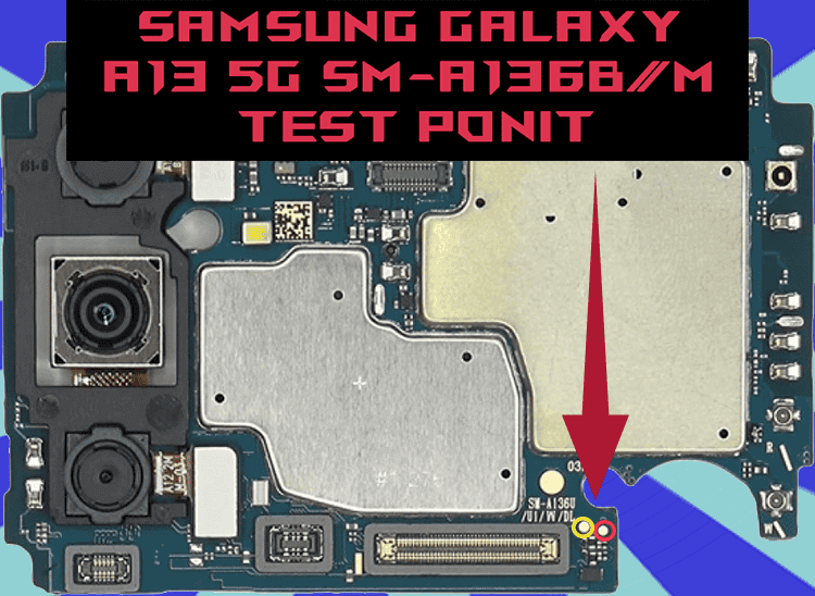
Samsung Galaxy A13 5G SM-A136B/M TEST POINT with the smartphone industry continually pushing the boundaries of what’s possible, understanding the intricacies of test points for the SM-A136B/M model becomes crucial for enthusiasts and technicians alike. In this article, we explore the world of the Samsung Galaxy A13 5G SM-A136B/M TEST POINT, exploring its significance and practical applications.
Unlocking the Secrets of SM-A136B/M TEST POINT: A Comprehensive Guide
Test points are specific points or connectors on electronic circuit boards or devices strategically placed to facilitate testing and debugging during manufacturing, repair, or quality control. They serve as access points for test equipment, such as oscilloscopes, multimeters, or JTAG (Joint Test Action Group) interfaces, allowing technicians and engineers to measure various electrical parameters and diagnose issues with the device’s hardware or firmware. These points are typically marked on the device’s PCB (Printed Circuit Board) and are crucial for ensuring the functionality and reliability of electronic devices.
Test points play a vital role in the electronics industry by simplifying the testing and validation of electronic components and devices. They allow for efficient and accurate troubleshooting, saving time and resources during the manufacturing and repair stages. Moreover, test points are essential for ensuring product quality and reliability, as they enable comprehensive testing to identify any manufacturing defects or anomalies early in the production process. In summary, test points are a fundamental aspect of electronics design and production, contributing to electronic devices’ overall performance and dependability.
SM-A136B/M Test Point Image